Conditions in the Intel 8087 floating-point chip's microcode
In the 1980s, if you wanted your computer to do floating-point calculations faster, you could buy the Intel 8087 floating-point coprocessor chip. Plugging it into your IBM PC would make operations up to 100 times faster, a big boost for spreadsheets and other number-crunching applications. The 8087 uses complicated algorithms to compute trigonometric, logarithmic, and exponential functions. These algorithms are implemented inside the chip in microcode. I'm part of a group that is reverse-engineering this microcode. In this post, I examine the 49 types of conditional tests that the 8087's microcode uses inside its algorithms. Some conditions are simple, such as checking if a number is zero or negative, while others are specialized, such as determining what direction to round a number.
To explore the 8087's circuitry, I opened up an 8087 chip and took numerous photos of the silicon die with a microscope. Around the edges of the die, you can see the hair-thin bond wires that connect the chip to its 40 external pins. The complex patterns on the die are formed by its metal wiring, as well as the polysilicon and silicon underneath. The bottom half of the chip is the "datapath", the circuitry that performs calculations on 80-bit floating point values. At the left of the datapath, a constant ROM holds important constants such as p. At the right are the eight registers that the programmer uses to hold floating-point values; in an unusual design decision, these registers are arranged as a stack.
The chip's instructions are defined by the large microcode ROM in the middle. To execute a floating-point instruction, the 8087 decodes the instruction and the microcode engine starts executing the appropriate micro-instructions from the microcode ROM. The microcode decode circuitry to the right of the ROM generates the appropriate control signals from each micro-instruction.1 The bus registers and control circuitry handle interactions with the main 8086 processor and the rest of the system.
The 8087's microcode
Executing an 8087 instruction such as arctan requires hundreds of internal steps to compute the result. These steps are implemented in microcode with micro-instructions specifying each step of the algorithm. (Keep in mind the difference between the assembly language instructions used by a programmer and the undocumented low-level micro-instructions used internally by the chip.) The microcode ROM holds 1648 micro-instructions, implementing the 8087's instruction set. Each micro-instruction is 16 bits long and performs a simple operation such as moving data inside the chip, adding two values, or shifting data. I'm working with the "Opcode Collective" to reverse engineer the micro-instructions and fully understand the microcode (link).
The microcode engine (below) controls the execution of micro-instructions, acting as the mini-CPU inside the 8087. Specifically, it generates an 11-bit micro-address, the address of a micro-instruction in the ROM. The microcode engine implements jumps, subroutine calls, and returns within the microcode. These jumps, subroutine calls, and returns are all conditional; the microcode engine will either perform the operation or skip it, depending on the value of a specified condition.
I'll write more about the microcode engine later, but I'll give an overview here. At the top, the Instruction Decode PLA2 decodes an 8087 instruction to determine the starting address in microcode. Below that, the Jump PLA holds microcode addresses for jumps and subroutine calls. Below this, six 11-bit registers implement the microcode stack, allowing six levels of subroutine calls inside the microcode. (Note that this stack is completely different from the 8087's register stack that holds eight floating-point values.) The stack registers have associated read/write circuitry. The incrementer adds one to the micro-address to step through the code. The engine also implements relative jumps, using an adder to add an offset to the current location. At the bottom, the address latch and drivers boost the 11-bit address output and send it to the microcode ROM.
Selecting a condition
A micro-instruction can say "jump ahead 5 micro-instructions if a register is zero" and the microcode engine will either perform the jump or ignore it, based on the register value. In the circuitry, the condition causes the microcode engine to either perform the jump or block the jump. But how does the hardware select one condition out of the large set of conditions?
Six bits of the micro-instruction can specify one of 64 conditions. A circuit similar to the idealized diagram below selects the specified condition. The key component is a multiplexer, represented by a trapezoid below. A multiplexer is a simple circuit that selects one of its four inputs. By arranging multiplexers in a tree, one of the 64 conditions on the left is selected and becomes the output, passed to the microcode engine.
For example, if bits J and K of the microcode are 00, the rightmost multiplexer will select the first input. If bits LM are 01, the middle multiplexer will select the second input, and if bits NO are 10, the left multiplexer will select its third input. The result is that condition 06 will pass through the tree and become the output.3 By changing the bits that control the multiplexers, any of the inputs can be used. (We've arbitrarily given the 16 microcode bits the letter names A through P.)
Physically, the conditions come from locations scattered across the die. For instance, conditions involving the opcode come from the instruction decoding part of the chip, while conditions involving a register are evaluated next to the register. It would be inefficient to run 64 wires for all the conditions to the microcode engine. The tree-based approach reduces the wiring since the "leaf" multiplexers can be located near the associated condition circuitry. Thus, only one wire needs to travel a long distance rather than multiple wires. In other words, the condition selection circuitry is distributed across the chip instead of being implemented as a centralized module.
Because the conditions don't always fall into groups of four, the actual implementation is slightly different from the idealized diagram above. In particular, the top-level multiplexer has five inputs, rather than four.4 Other multiplexers don't use all four inputs. This provides a better match between the physical locations of the condition circuits and the multiplexers. In total, 49 of the possible 64 conditions are implemented in the 8087.
The circuit that selects one of the four conditions is called a multiplexer. It is constructed from pass transistors, transistors that are configured to either pass a signal through or block it. To operate the multiplexer, one of the select lines is energized, turning on the corresponding pass transistor. This allows the selected input to pass through the transistor to the output, while the other inputs are blocked.
The diagram below shows how a multiplexer appears on the die. The pinkish regions are doped silicon. The white lines are polysilicon wires. When polysilicon crosses over doped silicon, a transistor is formed. On the left is a four-way multiplexer, constructed from four pass transistors. It takes inputs (black) for four conditions, numbered 38, 39, 3a, and 3b. There are four control signals (red) corresponding to the four combinations of bits N and O. One of the inputs will pass through a transistor to the output, selected by the active control signal. The right half contains the logic (four NOR gates and two inverters) to generate the control signals from the microcode bits. (Metal lines run horizontally from the logic to the control signal contacts, but I dissolved the metal for this photo.) Each multiplexer in the 8087 has a completely different layout, manually optimized based on the location of the signals and surrounding circuitry. Although the circuit for a multiplexer is regular (four transistors in parallel), the physical layout looks somewhat chaotic.
The 8087 uses pass transistors for many circuits, not just multiplexers. Circuits with pass transistors are different from regular logic gates because the pass transistors provide no amplification. Instead, signals get weaker as they go through pass transistors. To solve this problem, inverters or buffers are inserted into the condition tree to boost signals; they are omitted from the diagram above.
The conditions
Of the 8087's 49 different conditions, some are widely used in the microcode, while others are designed for a specific purpose and are only used once. The full set of conditions is described in a footnote7 but I'll give some highlights here.
Fifteen conditions examine the bits of the current instruction's opcode. This allows one microcode routine to handle a group of similar instructions and then change behavior based on the specific instruction. For example, conditions test if the instruction is multiplication, if the instruction is an FILD/FIST (integer load or store), or if the bottom bit of the opcode is set.5
The 8087 has three temporary registers--tmpA, tmpB, and tmpC--that hold values during computation. Various conditions examine the values in the tmpA and tmpB registers.6 In particular, the 8087 uses an interesting way to store numbers internally: each 80-bit floating-point value also has two "tag" bits. These bits are mostly invisible to the programmer and can be thought of as metadata. The tag bits indicate if a register is empty, contains zero, contains a "normal" number, or contains a special value such as NaN (Not a Number) or infinity. The 8087 uses the tag bits to optimize operations. The tags also detect stack overflow (storing to a non-empty stack register) or stack underflow (reading from an empty stack register).
Other conditions are highly specialized. For instance, one condition looks at the rounding mode setting and the sign of the value to determine if the value should be rounded up or down. Other conditions deal with exceptions such as numbers that are too small (i.e. denormalized) or numbers that lose precision. Another condition tests if two values have the same sign or not. Yet another condition tests if two values have the same sign or not, but inverts the result if the current instruction is subtraction. The simplest condition is simply "true", allowing an unconditional branch.
For flexibility, conditions can be "flipped", either jumping if the condition is true or jumping if the condition is false. This is controlled by bit P of the microcode. In the circuitry, this is implemented by a gate that XORs the P bit with the condition. The result is that the state of the condition is flipped if bit P is set.
For a concrete example of how conditions are used, consider the
microcode routine
that implements FCHS and FABS, the
instructions to change the sign and compute the absolute value, respectively.
These operations are almost the same (toggling the sign bit versus clearing the sign bit), so the same
microcode routine handles both instructions, with a jump instruction to handle the difference.
The FABS and FCHS instructions were designed with identical opcodes,
except that the bottom bit is set for FABS.
Thus, the microcode routine uses a condition that tests the bottom bit, allowing the routine to branch and
change its behavior for FABS vs FCHS.
Looking at the relevant micro-instruction, it has the hex value
0xc094, or in binary 110 000001 001010 0.
The first three bits (ABC=110) specify the relative jump operation (100 would jump to a fixed target and 101 would
perform a subroutine call.)
Bits D through I (000010) indicate the amount of the jump (+`).
Bits J through O (001010, hex 0a) specify the condition to test, in this case, the last bit of the instruction opcode.
The final bit (P) would toggle the condition if set, (i.e. jump if false).
Thus, for FABS, the jump instruction will jump ahead one micro-instruction.
This has the effect of skipping the next micro-instruction, which sets the appropriate sign bit for
FCHS.
Conclusions
The 8087 performs floating-point operations much faster than the 8086 by using special hardware, optimized for floating-point. The condition code circuitry is one example of this: the 8087 can test a complicated condition in a single operation. However, these complicated conditions make it much harder to understand the microcode. But by a combination of examining the circuitry and looking at the micocode, we're making progress. Thanks to the members of the "Opcode Collective" for their hard work, especially Smartest Blob and Gloriouscow.
For updates, follow me on Bluesky (@righto.com), Mastodon (@[email protected]), or RSS.
Notes and references
-
The section of the die that I've labeled "Microcode decode" performs some of the microcode decoding, but large parts of the decoding are scattered across the chip, close to the circuitry that needs the signals. This makes reverse-engineering the microcode much more difficult. I thought that understanding the microcode would be straightforward, just examining a block of decode circuitry. But this project turned out to be much more complicated and I need to reverse-engineer the entire chip. -
-
A PLA is a "Programmable Logic Array". It is a technique to implement logic functions with grids of transistors. A PLA can be used as a compressed ROM, holding data in a more compact representation. (Saving space was very important in chips of this era.) In the 8087, PLAs are used to hold tables of microcode addresses. -
-
Note that the multiplexer circuit selects the condition corresponding to the binary value of the bits. In the example, bits 000110 (0x06) select condition 06. -
-
The five top-level multiplexer inputs correspond to bit patterns 00, 011, 10, 110, and 111. That is, two inputs depend on bits J and K, while three inputs depend on bits J, K, and L. The bit pattern 010 is unused, corresponding to conditions 0x10 through 0x17, which aren't implemented. -
-
The 8087 acts as a co-processor with the 8086 processor. The 8086 instruction set is designed so instructions with a special "ESCAPE" sequence in the top 5 bits are processed by the co-processor, in this case the 8087. Thus, the 8087 receives a 16-bit instruction, but only the bottom 11 bits are usable. For a memory operation, the second byte of the instruction is an 8086-style ModR/M byte. For instructions that don't access memory, the second byte specifies more of the instruction and sometimes specifies the stack register to use for the instruction.
The relevance of this is that the 8087's microcode engine uses the 11 bits of the instruction to determine which microcode routine to execute. The microcode also uses various condition codes to change behavior depending on different bits of the instruction. -
-
There is a complication with the tmpA and tmpB registers: they can be swapped with the micro-instruction "ABC.EF". The motivation behind this is that if you have two arguments, you can use a micro-subroutine to load an argument into tmpA, swap the registers, and then use the same subroutine to load the second argument into tmpA. The result is that the two arguments end up in tmpB and tmpA without any special coding in the subroutine.
The implementation doesn't physically swap the registers, but renames them internally, which is much more efficient. A flip-flop is toggled every time the registers are swapped. If the flip-flop is set, a request goes to one register, while if the flip-flop is clear, a request goes to the other register. (Many processors use the same trick. For instance, the Intel 8080 has an instruction to exchange the DE and HL registers. The Z80 has an instruction to swap register banks. In both cases, a flip-flop renames the registers, so the data doesn't need to move.) -
-
The table below is the real meat of this post, the result of much circuit analysis. These details probably aren't interesting to most people, so I've relegated the table to a footnote. Descriptions in italics are provided by Smartest Blob based on examination of the microcode. Grayed-out lines are unused conditions.
The table has five sections, corresponding to the 5 inputs to the top-level condition multiplexer. These inputs come from different parts of the chip, so the sections correspond to different categories of conditions.
The first section consists of instruction parsing, with circuitry near the microcode engine. The description shows the 11-bit opcode pattern that triggers the condition, with 0 bits and 1 bits as specified, and X indicating a "don't care" bit that can be 0 or 1. Where simpler, I list the relevant instructions instead.
The next section indicates conditions on the exponent. I am still investigating these conditions, so the descriptions are incomplete. The third section is conditions on the temporary registers or conditions related to the control register. These circuits are to the right of the microcode ROM.
Conditions in the fourth section examine the floating-point bus, with circuitry near the bottom of the chip. Conditions 34 and 35 use a special 16-bit bidirectional shift register, at the far right of the chip. The top bit from the floating-point bus is shifted in. Maybe this shift register is used for CORDIC calculations? The conditions in the final block are miscellaneous, including the always-true condition 3e, which is used for unconditional jumps.
Cond. Description 00 not XXX 11XXXXXX 01 1XX 11XXXXXX 02 0XX 11XXXXXX 03 X0X XXXXXXXX 04 not cond 07 or 1XX XXXXXXXX 05 not FLD/FSTP temp-real or BCD 06 110 xxxxxxxx or 111 xx0xxxxx 07 FLD/FSTP temp-real 08 FBLD/FBSTP 09 0a XXX XXXXXXX1 0b XXX XXXX1XXX 0c FMUL 0d FDIV FDIVR 0e FADD FCOM FCOMP FCOMPP FDIV FDIVR FFREE FLD FMUL FST FSTP FSUB FSUBR FXCH 0f FCOM FCOMP FCOMPP FTST 10 11 12 13 14 15 16 17 18 exponent condition 19 exponent condition 1a exponent condition 1b exponent condition 1c exponent condition 1d exponent condition 1e eight exponent zero bits 1f exponent condition 20 tmpA tag ZERO 21 tmpA tag SPECIAL 22 tmpA tag VALID 23 stack overflow 24 tmpB tag ZERO 25 tmpB tag SPECIAL 26 tmpB tag VALID 27 st(i) doesn't exist (A)? 28 tmpA sign 29 tmpB top bit 2a tmpA zero 2b tmpA top bit 2c Control Reg bit 12: infinity control 2d round up/down 2e unmasked interrupt 2f DE (denormalized) interrupt 30 top reg bit 31 32 reg bit 64 33 reg bit 63 34 Shifted top bits, all zero 35 Shifted top bits, one out 36 37 38 const latch zero 39 tmpA vs tmpB sign, flipped for subtraction 3a precision exception 3b tmpA vs tmpB sign 3c 3d 3e unconditional 3f This table is under development and undoubtedly has errors. -
The stack circuitry of the Intel 8087 floating point chip, reverse-engineered
Early microprocessors were very slow when operating with floating-point numbers. But in 1980, Intel introduced the 8087 floating-point coprocessor, performing floating-point operations up to 100 times faster. This was a huge benefit for IBM PC applications such as AutoCAD, spreadsheets, and flight simulators. The 8087 was so effective that today's computers still use a floating-point system based on the 8087.1
The 8087 was an extremely complex chip for its time, containing somewhere between 40,000 and 75,000 transistors, depending on the source.2 To explore how the 8087 works, I opened up a chip and took numerous photos of the silicon die with a microscope. Around the edges of the die, you can see the hair-thin bond wires that connect the chip to its 40 external pins. The complex patterns on the die are formed by its metal wiring, as well as the polysilicon and silicon underneath. The bottom half of the chip is the "datapath", the circuitry that performs calculations on 80-bit floating point values. At the left of the datapath, a constant ROM holds important constants such as p. At the right are the eight registers that form the stack, along with the stack control circuitry.
The chip's instructions are defined by the large microcode ROM in the middle. This ROM is very unusual; it is semi-analog, storing two bits per transistor by using four transistor sizes. To execute a floating-point instruction, the 8087 decodes the instruction and the microcode engine starts executing the appropriate micro-instructions from the microcode ROM. The decode circuitry to the right of the ROM generates the appropriate control signals from each micro-instruction. The bus registers and control circuitry handle interactions with the main 8086 processor and the rest of the system. Finally, the bias generator uses a charge pump to create a negative voltage to bias the chip's substrate, the underlying silicon.
The stack registers and control circuitry (in red above) are the subject of this blog post. Unlike most processors, the 8087 organizes its registers in a stack, with instructions operating on the top of the stack. For instance, the square root instruction replaces the value on the top of the stack with its square root. You can also access a register relative to the top of the stack, for instance, adding the top value to the value two positions down from the top. The stack-based architecture was intended to improve the instruction set, simplify compiler design, and make function calls more efficient, although it didn't work as well as hoped.
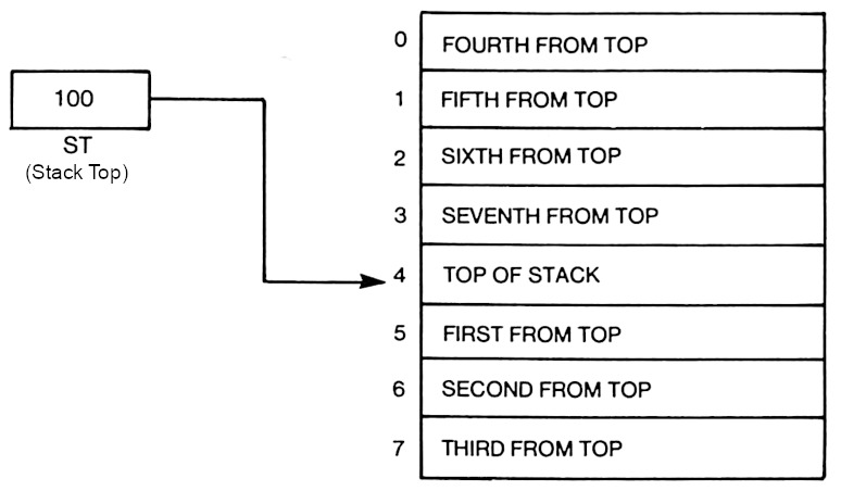
The diagram above shows how the stack operates. The stack consists of eight registers, with the Stack Top (ST) indicating the current top of the stack. To push a floating-point value onto the stack, the Stack Top is decremented and then the value is stored in the new top register. A pop is performed by copying the value from the stack top and then incrementing the Stack Top. In comparison, most processors specify registers directly, so register 2 is always the same register.
The registers
The stack registers occupy a substantial area on the die of the 8087 because floating-point numbers take many bits. A floating-point number consists of a fractional part (sometimes called the mantissa or significand), along with the exponent part; the exponent allows floating-point numbers to cover a range from extremely small to extremely large. In the 8087, floating-point numbers are 80 bits: 64 bits of significand, 15 bits of exponent, and a sign bit. An 80-bit register was very large in the era of 8-bit or 16-bit computers; the eight registers in the 8087 would be equivalent to 40 registers in the 8086 processor.
The registers store each bit in a static RAM cell. Each cell has two inverters connected in a loop. This circuit forms a stable feedback loop, with one inverter on and one inverter off. Depending on which inverter is on, the circuit stores a 0 or a 1. To write a new value into the circuit, one of the lines is pulled low, flipping the loop into the desired state. The trick is that each inverter uses a very weak transistor to pull the output high, so its output is easily overpowered to change the state.
These inverter pairs are arranged in an 8 x 80 grid that implements eight words of 80 bits. Each of the 80 rows has two bitlines that provide access to a bit. The bitlines provide both read and write access to a bit; the pair of bitlines allows either inverter to be pulled low to store the desired bit value. Eight vertical wordlines enable access to one word, one column of 80 bits. Each wordline turns on 160 pass transistors, connecting the bitlines to the inverters in the selected column. Thus, when a wordline is enabled, the bitlines can be used to read or write that word.
Although the chip looks two-dimensional, it actually consists of multiple layers. The bottom layer is silicon. The pinkish regions below are where the silicon has been "doped" to change its electrical properties, making it an active part of the circuit. The doped silicon forms a grid of horizontal and vertical wiring, with larger doped regions in the middle. On top of the silicon, polysilicon wiring provides two functions. First, it provides a layer of wiring to connect the circuit. But more importantly, when polysilicon crosses doped silicon, it forms a transistor. The polysilicon provides the gate, turning the transistor on and off. In this photo, the polysilicon is barely visible, so I've highlighted part of it in red. Finally, horizontal metal wires provide a third layer of interconnecting wiring. Normally, the metal hides the underlying circuitry, so I removed the metal with acid for this photo. I've drawn blue lines to represent the metal layer. Contacts provide connections between the various layers.
The layers combine to form the inverters and selection transistors of a memory cell, indicated with the dotted line below. There are six transistors (yellow), where polysilicon crosses doped silicon. Each inverter has a transistor that pulls the output low and a weak transistor to pull the output high. When the word line (vertical polysilicon) is active, it connects the selected inverters to the bit lines (horizontal metal) through the two selection transistors. This allows the bit to be read or written.
Each register has two tag bits associated with it, an unusual form of metadata to indicate if the register is empty, contains zero, contains a valid value, or contains a special value such as infinity. The tag bits are used to optimize performance internally and are mostly irrelevant to the programmer. As well as being accessed with a register, the tag bits can be accessed in parallel as a 16-bit "Tag Word". This allows the tags to be saved or loaded as part of the 8087's state, for instance, during interrupt handling.
The decoder
The decoder circuit, wedged into the middle of the register file, selects one of the registers. A register is specified internally with a 3-bit value. The decoder circuit energizes one of the eight register select lines based on this value.
The decoder circuitry is straightforward: it has eight 3-input NOR gates to match one of the eight bit patterns. The select line is then powered through a high-current driver that uses large transistors. (In the photo below, you can compare the large serpentine driver transistors to the small transistors in a bit cell.)
The decoder has an interesting electrical optimization. As shown earlier, the register select lines are eight polysilicon lines running vertically, the length of the register file. Unfortunately, polysilicon has fairly high resistance, better than silicon but much worse than metal. The problem is that the resistance of a long polysilicon line will slow down the system. That is, the capacitance of transistor gates in combination with high resistance causes an RC (resistive-capacitive) delay in the signal.
The solution is that the register select lines also run in the metal layer, a second set of lines immediately to the right of the register file. These lines branch off from the register file about 1/3 of the way down, run to the bottom, and then connect back to the polysilicon select lines at the bottom. This reduces the maximum resistance through a select line, increasing the speed.
The stack control circuitry
A stack needs more control circuitry than a regular register file, since the circuitry must keep track of the position of the top of the stack.3 The control circuitry increments and decrements the top of stack (TOS) pointer as values are pushed or popped (purple).4 Moreover, an 8087 instruction can access a register based on its offset, for instance the third register from the top. To support this, the control circuitry can temporarily add an offset to the top of stack position (green). A multiplexer (red) selects either the top of stack or the adder output, and feeds it to the decoder (blue), which selects one of the eight stack registers in the register file (yellow), as described earlier.
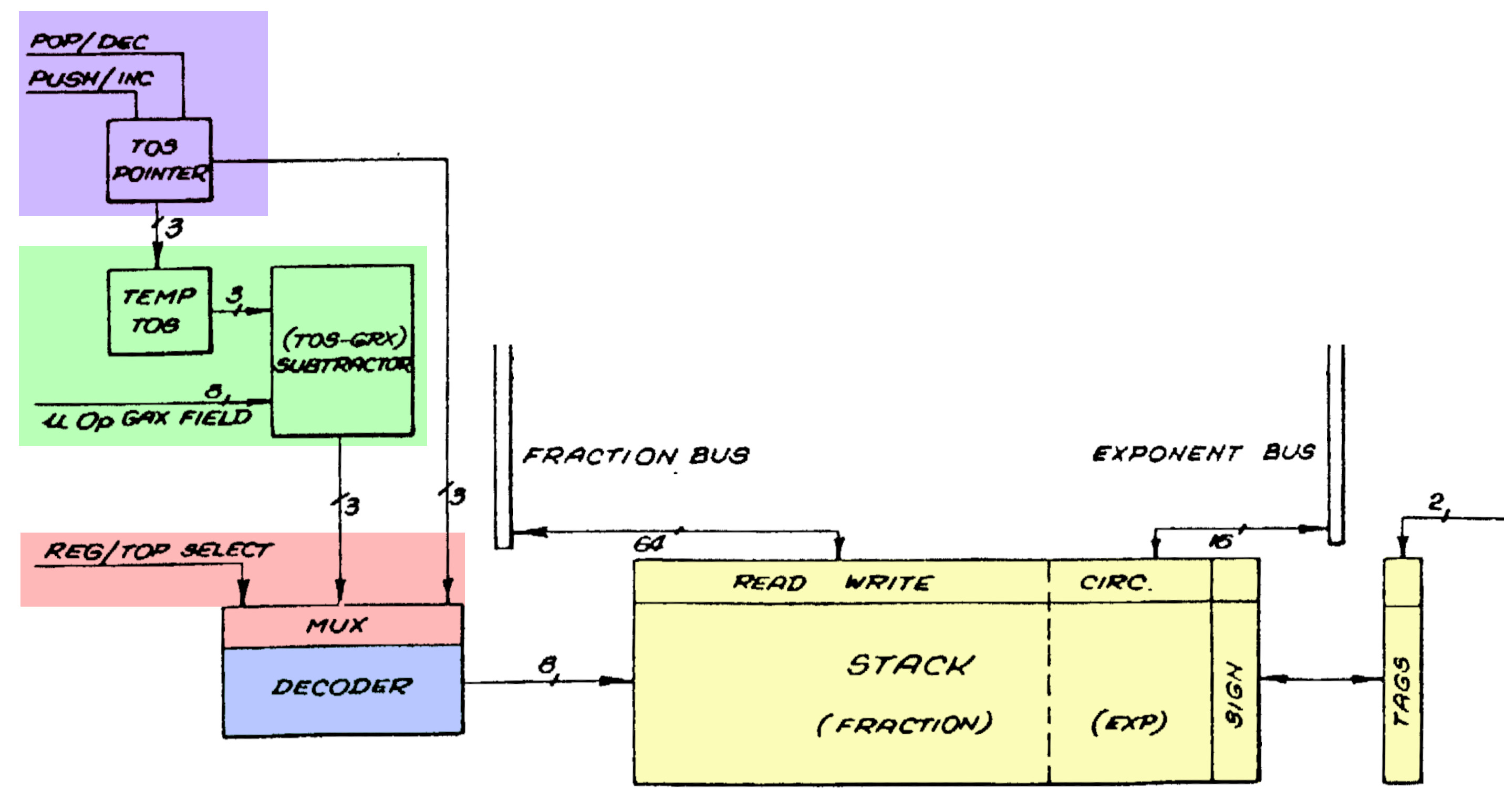
The physical implementation of the stack circuitry is shown below. The logic at the top selects the stack operation based on the 16-bit micro-instruction.5 Below that are the three latches that hold the top of stack value. (The large white squares look important, but they are simply "jumpers" from the ground line to the circuitry, passing under metal wires.)
The three-bit adder is at the bottom, along with the multiplexer. You might expect the adder to use a simple "full adder" circuit. Instead, it is a faster carry-lookahead adder. I won't go into details here, but the summary is that at each bit position, an AND gate produces a Carry Generate signal while an XOR gate produces a Carry Propagate signal. Logic gates combine these signals to produce the output bits in parallel, avoiding the slowdown of the carry rippling through the bits.
The incrementer/decrementer uses a completely different approach. Each of the three bits uses a toggle flip-flop. A few logic gates determine if each bit should be toggled or should keep its previous value. For instance, when incrementing, the top bit is toggled if the lower bits are 11 (e.g. incrementing from 011 to 100). For decrementing, the top bit is toggled if the lower bits are 00 (e.g. 100 to 011). Simpler logic determines if the middle bit should be toggled. The bottom bit is easier, toggling every time whether incrementing or decrementing.
The schematic below shows the circuitry for one bit of the stack. Each bit is implemented with a moderately complicated flip-flop that can be cleared, loaded with a value, or toggled, based on control signals from the microcode. The flip-flop is constructed from two set-reset (SR) latches. Note that the flip-flop outputs are crossed when fed back to the input, providing the inversion for the toggle action. At the right, the multiplexer selects either the register value or the sum from the adder (not shown), generating the signals to the decoder.
Drawbacks of the stack approach
According to the designers of the 8087,7 the main motivation for using a stack rather than a flat register set was that instructions didn't have enough bits to address multiple register operands. In addition, a stack has "advantages over general registers for expression parsing and nested function calls." That is, a stack works well for a mathematical expression since sub-expressions can be evaluated on the top of the stack. And for function calls, you avoid the cost of saving registers to memory, since the subroutine can use the stack without disturbing the values underneath. At least that was the idea.
The main problem is "stack overflow". The 8087's stack has eight entries, so if you push a ninth value onto the stack, the stack will overflow. Specifically, the top-of-stack pointer will wrap around, obliterating the bottom value on the stack. The 8087 is designed to detect a stack overflow using the register tags: pushing a value to a non-empty register triggers an invalid operation exception.6
The designers expected that stack overflow would be rare and could be handled by the operating system (or library code). After detecting a stack overflow, the software should dump the existing stack to memory to provide the illusion of an infinite stack. Unfortunately, bad design decisions made it difficult "both technically and commercially" to handle stack overflow.
One of the 8087's designers (Kahan) attributes the 8087's stack problems to the time difference between California, where the designers lived, and Israel, where the 8087 was implemented. Due to a lack of communication, each team thought the other was implementing the overflow software. It wasn't until the 8087 was in production that they realized that "it might not be possible to handle 8087 stack underflow/overflow in a reasonable way. It's not impossible, just impossible to do it in a reasonable way."
As a result, the stack was largely a problem rather than a solution.
Most 8087 software saved the full stack to memory before performing
a function call, creating more memory traffic.
Moreover, compilers turned out to work better with regular registers than a stack,
so compiler writers awkwardly used the stack to emulate regular registers.
The GCC compiler reportedly needs 3000 lines of extra code to support the x87 stack.
In the 1990s, Intel introduced a new floating-point system called SSE, followed by AVX in 2011. These systems use regular (non-stack) registers and provide parallel operations for higher performance, making the 8087's stack instructions largely obsolete.
The success of the 8087
At the start, Intel was unenthusiastic about producing the 8087, viewing it as unlikely to be a success. John Palmar, a principal architect of the chip, had little success convincing skeptical Intel management that the market for the 8087 was enormous. Eventually, he said, "I'll tell you what. I'll relinquish my salary, provided you'll write down your number of how many you expect to sell, then give me a dollar for every one you sell beyond that."7 Intel didn't agree to the deal--which would have made a fortune for Palmer--but they reluctantly agreed to produce the chip.
Intel's Santa Clara engineers shunned the 8087, considering it unlikely to work: the 8087 would be two to three times more complex than the 8086, with a die so large that a wafer might not have a single working die. Instead, Rafi Nave, at Intel's Israel site, took on the risky project: "Listen, everybody knows it's not going to work, so if it won't work, I would just fulfill their expectations or their assessment. If, by chance, it works, okay, then we'll gain tremendous respect and tremendous breakthrough on our abilities."
A small team of seven engineers developed the 8087 in Israel. They designed the chip on Mylar sheets: a millimeter on Mylar represented a micron on the physical chip. The drawings were then digitized on a Calma system by clicking on each polygon to create the layout. When the chip was moved into production, the yield was very low but better than feared: two working dies per four-inch wafer.
The 8087 ended up being a large success, said to have been Intel's most profitable product line at times. The success of the 8087 (along with the 8088) cemented the reputation of Intel Israel, which eventually became Israel's largest tech employer. The benefits of floating-point hardware proved to be so great that Intel integrated the floating-point unit into later processors starting with the 80486 (1989). Nowadays, most modern computers, from cellphones to mainframes, provide floating point based on the 8087, so I consider the 8087 one of the most influential chips ever created.
For more, follow me on Bluesky (@righto.com), Mastodon (@[email protected]), or RSS. I wrote some articles about the 8087 a few years ago, including the die, the ROM, the bit shifter, and the constants, so you may have seen some of this material before.
Notes and references
-
Most computers now use the IEEE 754 floating-point standard, which is based on the 8087. This standard has been awarded a milestone in computation. -
-
Curiously, reliable sources differ on the number of transistors in the 8087 by almost a factor of 2. Intel says 40,000, as does designer William Kahan (link). But in A Numeric Data Processor, designers Rafi Nave and John Palmer wrote that the chip contains "the equivalent of over 65,000 devices" (whatever "equivalent" means). This number is echoed by a contemporary article in Electronics (1980) that says "over 65,000 H-MOS transistors on a 78,000-mil2 die." Many other sources, such as Upgrading & Repairing PCs, specify 45,000 transistors. Designer Rafi Nave stated that the 8087 has 63,000 or 64,000 transistors if you count the ROM transistors directly, but if you count ROM transistors as equivalent to two transistors, then you get about 75,000 transistors. -
-
The 8087 has a 16-bit Status Word that contains the stack top pointer, exception flags, the four-bit condition code, and other values. Although the Status Word appears to be a 16-bit register, it is not implemented as a register. Instead, parts of the Status Word are stored in various places around the chip: the stack top pointer is in the stack circuitry, the exception flags are part of the interrupt circuitry, the condition code bits are next to the datapath, and so on. When the Status Word is read or written, these various circuits are connected to the 8087's internal data bus, making the Status Word appear to be a monolithic entity. Thus, the stack circuitry includes support for reading and writing it. -
-
Intel filed several patents on the 8087, including Numeric data processor, another Numeric data processor, Programmable bidirectional shifter, Fraction bus for use in a numeric data processor, and System bus arbitration, circuitry and methodology. -
-
I started looking at the stack in detail to reverse engineer the micro-instruction format and determine how the 8087's microcode works. I'm working with the "Opcode Collective" on Discord on this project, but progress is slow due to the complexity of the micro-instructions. -
-
The 8087 detects stack underflow in a similar manner. If you pop more values from the stack than are present, the tag will indicate that the register is empty and shouldn't be accessed. This triggers an invalid operation exception. -
-
The 8087 is described in detail in The 8086 Family User's Manual, Numerics Supplement. An overview of the stack is on page 60 of The 8087 Primer by Palmer and Morse. More details are in Kahan's On the Advantages of the 8087's Stack, an unpublished course note (maybe for CS 279?) with a date of Nov 2, 1990 or perhaps August 23, 1994. Kahan discusses why the 8087's design makes it hard to handle stack overflow in How important is numerical accuracy, Dr. Dobbs, Nov. 1997. Another information source is the Oral History of Rafi Nave --
Unusual circuits in the Intel 386's standard cell logic
I've been studying the standard cell circuitry in the Intel 386 processor recently. The 386, introduced in 1985, was Intel's most complex processor at the time, containing 285,000 transistors. Intel's existing design techniques couldn't handle this complexity and the chip began to fall behind schedule. To meet the schedule, the 386 team started using a technique called standard cell logic. Instead of laying out each transistor manually, the layout process was performed by a computer.
The idea behind standard cell logic is to create standardized circuits (standard cells) for each type of logic element, such as an inverter, NAND gate, or latch. You feed your circuit description into software that selects the necessary cells, positions these cells into columns, and then routes the wiring between the cells. This "automatic place and route" process creates the chip layout much faster than manual layout. However, switching to standard cells was a risky decision since if the software couldn't create a dense enough layout, the chip couldn't be manufactured. But in the end, the 386 finished ahead of schedule, an almost unheard-of accomplishment.1
The 386's standard cell circuitry contains a few circuits that I didn't expect. In this blog post, I'll take a quick look at some of these circuits: surprisingly large multiplexers, a transistor that doesn't fit into the standard cell layout, and inverters that turned out not to be inverters. (If you want more background on standard cells in the 386, see my earlier post, "Reverse engineering standard cell logic in the Intel 386 processor".)
The photo below shows the 386 die with the automatic-place-and-route regions highlighted; I'm focusing on the red region in the lower right. These blocks of logic have cells arranged in rows, giving them a characteristic striped appearance. The dark stripes are the transistors that make up the logic gates, while the lighter regions between the stripes are the "routing channels" that hold the wiring that connects the cells. In comparison, functional blocks such as the datapath on the left and the microcode ROM in the lower right were designed manually to optimize density and performance, giving them a more solid appearance.
As for other features on the chip, the black circles around the border are bond wire connections that go to the chip's external pins. The chip has two metal layers, a small number by modern standards, but a jump from the single metal layer of earlier processors such as the 286. (Providing two layers of metal made automated routing practical: one layer can hold horizontal wires while the other layer can hold vertical wires.) The metal appears white in larger areas, but purplish where circuitry underneath roughens its surface. The underlying silicon and the polysilicon wiring are obscured by the metal layers.
The giant multiplexers
The standard cell circuitry that I'm examining (red box above) is part of the control logic that selects registers while executing an instruction. You might think that it is easy to select which registers take part in an instruction, but due to the complexity of the x86 architecture, it is more difficult. One problem is that a 32-bit register such as EAX can also be treated as the 16-bit register AX, or two 8-bit registers AH and AL. A second problem is that some instructions include a "direction" bit that switches the source and destination registers. Moreover, sometimes the register is specified by bits in the instruction, but in other cases, the register is specified by the microcode. Due to these factors, selecting the registers for an operation is a complicated process with many cases, using control bits from the instruction, from the microcode, and from other sources.
Three registers need to be selected for an operation--two source registers and a destination register--and there are about 17 cases that need to be handled. Registers are specified with 7-bit control signals that select one of the 30 registers and control which part of the register is accessed. With three control signals, each 7 bits wide, and about 17 cases for each, you can see that the register control logic is large and complicated. (I wrote more about the 386's registers here.)
I'm still reverse engineering the register control logic, so I won't go into details. Instead, I'll discuss how the register control circuit uses multiplexers, implemented with standard cells. A multiplexer is a circuit that combines multiple input signals into a single output by selecting one of the inputs.2 A multiplexer can be implemented with logic gates, for instance, by ANDing each input with the corresponding control line, and then ORing the results together. However, the 386 uses a different approach--CMOS switches--that avoids a large AND/OR gate.
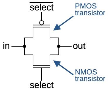
The schematic above shows how a CMOS switch is constructed from two MOS transistors. When the two transistors are on, the output is connected to the input, but when the two transistors are off, the output is isolated. An NMOS transistor is turned on when its input is high, but a PMOS transistor is turned on when its input is low. Thus, the switch uses two control inputs, one inverted. The motivation for using two transistors is that an NMOS transistor is better at pulling the output low, while a PMOS transistor is better at pulling the output high, so combining them yields the best performance.3 Unlike a logic gate, the CMOS switch has no amplification, so a signal is weakened as it passes through the switch. As will be seen below, inverters can be used to amplify the signal.
The image below shows how CMOS switches appear under the microscope. This image is very hard to interpret because the two layers of metal on the 386 are packed together densely, but you can see that some wires run horizontally and others run vertically. The bottom layer of metal (called M1) runs vertically in the routing area, as well as providing internal wiring for a cell. The top layer of metal (M2) runs horizontally; unlike M1, the M2 wires can cross a cell. The large circles are vias that connect the M1 and M2 layers, while the small circles are connections between M1 and polysilicon or M1 and silicon. The central third of the image is a column of standard cells with two CMOS switches outlined in green. The cells are bordered by the vertical ground rail and +5V rail that power the cells. The routing areas are on either side of the cells, holding the wiring that connects the cells.
Removing the metal layers reveals the underlying silicon with a layer of polysilicon wiring on top. The doped silicon regions show up as dark outlines. I've drawn the polysilicon in green; it forms a transistor (brighter green) when it crosses doped silicon. The metal ground and power lines are shown in blue and red, respectively, with other metal wiring in purple. The black dots are vias between layers. Note how metal wiring (purple) and polysilicon wiring (green) are combined to route signals within the cell. Although this standard cell is complicated, the important thing is that it only needs to be designed once. The standard cells for different functions are all designed to have the same width, so the cells can be arranged in columns, snapped together like Lego bricks.
To summarize, this switch circuit allows the input to be connected to the output or disconnected, controlled by the select signal. This switch is more complicated than the earlier schematic because it includes two inverters to amplify the signal. The data input and the two select lines are connected to the polysilicon (green); the cell is designed so these connections can be made on either side. At the top, the input goes through a standard two-transistor inverter. The lower left has two transistors, combining the NMOS half of an inverter with the NMOS half of the switch. A similar circuit on the right combines the PMOS part of an inverter and switch. However, because PMOS transistors are weaker, this part of the circuit is duplicated.
A multiplexer is constructed by combining multiple switches, one for each input. Turning on one switch will select the corresponding input. For instance, a four-to-one multiplexer has four switches, so it can select one of the four inputs.
The schematic above shows a hypothetical multiplexer with four inputs. One optimization is that if an input is always 0, the PMOS transistor can be omitted. Likewise, if an input is always 1, the NMOS transistor can be omitted. One set of select lines is activated at a time to select the corresponding input. The pink circuit selects 1, green selects input A, yellow selects input B, and blue selects 0. The multiplexers in the 386 are similar, but have more inputs.
The diagram below shows how much circuitry is devoted to multiplexers in this block of standard cells. The green, purple, and red cells correspond to the multiplexers driving the three register control outputs. The yellow cells are inverters that generate the inverted control signals for the CMOS switches. This diagram also shows how the automatic layout of cells results in a layout that appears random.
The misplaced transistor
The idea of standard-cell logic is that standardized cells are arranged in columns. The space between the cells is the "routing channel", holding the wiring that links the cells. The 386 circuitry follows this layout, except for one single transistor, sitting between two columns of cells.
I wrote some software tools to help me analyze the standard cells. Unfortunately, my tools assumed that all the cells were in columns, so this one wayward transistor caused me considerable inconvenience.
The transistor turns out to be a PMOS transistor, pulling a signal high as part of a multiplexer. But why is this transistor out of place? My hypothesis is that the transistor is a bug fix. Regenerating the cell layout was very costly, taking many hours on an IBM mainframe computer. Presumably, someone found that they could just stick the necessary transistor into an unused spot in the routing channel, manually add the necessary wiring, and avoid the delay of regenerating all the cells.
The fake inverter
The simplest CMOS gate is the inverter, with an NMOS transistor to pull the output low and a PMOS transistor to pull the output high. The standard cell circuitry that I examined contains over a hundred inverters of various sizes. (Performance is improved by using inverters that aren't too small but also aren't larger than necessary for a particular circuit. Thus, the standard cell library includes inverters of multiple sizes.)
The image below shows a medium-sized standard-cell inverter under the microscope. For this image, I removed the two metal layers with acid to show the underlying polysilicon (bright green) and silicon (gray). The quality of this image is poor--it is difficult to remove the metal without destroying the polysilicon--but the diagram below should clarify the circuit. The inverter has two transistors: a PMOS transistor connected to +5 volts to pull the output high when the input is 0, and an NMOS transistor connected to ground to pull the output low when the input is 1. (The PMOS transistor needs to be larger because PMOS transistors don't function as well as NMOS transistors due to silicon physics.)
The polysilicon input line plays a key role: where it crosses the doped silicon, a transistor gate is formed. To make the standard cell more flexible, the input to the inverter can be connected on either the left or the right; in this case, the input is connected on the right and there is no connection on the left. The inverter's output can be taken from the polysilicon on the upper left or the right, but in this case, it is taken from the upper metal layer (not shown). The power, ground, and output lines are in the lower metal layer, which I have represented by the thin red, blue, and yellow lines. The black circles are connections between the metal layer and the underlying silicon.
This inverter appears dozens of times in the circuitry. However, I came across a few inverters that didn't make sense. The problem was that the inverter's output was connected to the output of a multiplexer. Since an inverter is either on or off, its value would clobber the output of the multiplexer.4 This didn't make any sense. I double- and triple-checked the wiring to make sure I hadn't messed up. After more investigation, I found another problem: the input to a "bad" inverter didn't make sense either. The input consisted of two signals shorted together, which doesn't work.
Finally, I realized what was going on. A "bad inverter" has the exact silicon layout of an inverter, but it wasn't an inverter: it was independent NMOS and PMOS transistors with separate inputs. Now it all made sense. With two inputs, the input signals were independent, not shorted together. And since the transistors were controlled separately, the NMOS transistor could pull the output low in some circumstances, the PMOS transistor could pull the output high in other circumstances, or both transistors could be off, allowing the multiplexer's output to be used undisturbed. In other words, the "inverter" was just two more cases for the multiplexer.
If you compare the "bad inverter" cell below with the previous cell, they look almost the same, but there are subtle differences. First, the gates of the two transistors are connected in the real inverter, but disconnected by a small gap in the transistor pair. I've indicated this gap in the photo above; it is hard to tell if the gap is real or just an imaging artifact, so I didn't spot it. The second difference is that the "fake" inverter has two input connections, one to each transistor, while the inverter has a single input connection. Unfortunately, I assumed that the two connections were just a trick to route the signal across the inverter without requiring an extra wire. In total, this cell was used 32 times as a real inverter and 9 times as independent transistors.
Conclusions
Standard cell logic and automatic place and route have a long history before the 386, back to the early 1970s, so this isn't an Intel invention.5 Nonetheless, the 386 team deserves the credit for deciding to use this technology at a time when it was a risky decision. They needed to develop custom software for their placing and routing needs, so this wasn't a trivial undertaking. This choice paid off and they completed the 386 ahead of schedule. The 386 ended up being a huge success for Intel, moving the x86 architecture to 32 bits and defining the dominant computer architecture for the rest of the 20th century.
If you're interested in standard cell logic, I also wrote about standard cell logic in an IBM chip. I plan to write more about the 386, so follow me on Mastodon, Bluesky, or RSS for updates. Thanks to Pat Gelsinger and Roxanne Koester for providing helpful papers.
For more on the 386 and other chips, follow me on Mastodon (@[email protected]), Bluesky (@righto.com), or RSS. (I've given up on Twitter.) If you want to read more about the 386, I've written about the clock pin, prefetch queue, die versions, packaging, and I/O circuits.
Notes and references
-
The decision to use automatic place and route is described on page 13 of the Intel 386 Microprocessor Design and Development Oral History Panel, a very interesting document on the 386 with discussion from some of the people involved in its development. -
-
Multiplexers often take a binary control signal to select the desired input. For instance, an 8-to-1 multiplexer selects one of 8 inputs, so a 3-bit control signal can specify the desired input. The 386's multiplexers use a different approach with one control signal per input. One of the 8 control signals is activated to select the desired input. This approach is called a "one-hot encoding" since one control line is activated (hot) at a time. -
-
Some chips, such as the MOS Technology 6502 processor, are built with NMOS technology, without PMOS transistors. Multiplexers in the 6502 use a single NMOS transistor, rather than the two transistors in the CMOS switch. However, the performance of the switch is worse. -
-
One very common circuit in the 386 is a latch constructed from an inverter loop and a switch/multiplexer. The inverter's output and the switch's output are connected together. The trick, however, is that the inverter is constructed from special weak transistors. When the switch is disabled, the inverter's weak output is sufficient to drive the loop. But to write a value into the latch, the switch is enabled and its output overpowers the weak inverter.
The point of this is that there are circuits where an inverter and a multiplexer have their outputs connected. However, the inverter must be constructed with special weak transistors, which is not the situation that I'm discussing. -
-
I'll provide more history on standard cells in this footnote. RCA patented a bipolar standard cell in 1971, but this was a fixed arrangement of transistors and resistors, more of a gate array than a modern standard cell. Bell Labs researched standard cell layout techniques in the early 1970s, calling them Polycells, including a 1973 paper by Brian Kernighan. By 1979, A Guide to LSI Implementation discussed the standard cell approach and it was described as well-known in this patent application. Even so, Electronics called these design methods "futuristic" in 1980.
Standard cells became popular in the mid-1980s as faster computers and improved design software made it practical to produce semi-custom designs that used standard cells. Standard cells made it to the cover of Digital Design in August 1985, and the article inside described numerous vendors and products. Companies like Zymos and VLSI Technology (VTI) focused on standard cells. Traditional companies such as Texas Instruments, NCR, GE/RCA, Fairchild, Harris, ITT, and Thomson introduced lines of standard cell products in the mid-1980s. -
Here be dragons: Preventing static damage, latchup, and metastability in the 386
I've been reverse-engineering the Intel 386 processor (from 1985), and I've come across some interesting circuits for the chip's input/output (I/O) pins. Since these pins communicate with the outside world, they face special dangers: static electricity and latchup can destroy the chip, while metastability can cause serious malfunctions. These I/O circuits are completely different from the logic circuits in the 386, and I've come across a previously-undescribed flip-flop circuit, so I'm venturing into uncharted territory. In this article, I take a close look at how the I/O circuitry protects the 386 from the "dragons" that can destroy it.
The photo above shows the die of the 386 under a microscope. The dark, complex patterns arranged in rectangular regions arise from the two layers of metal that connect the circuits on the 386 chip. Not visible are the transistors, formed from silicon and polysilicon and hidden beneath the metal. Around the perimeter of this fingernail-sized silicon die, 141 square bond pads provide the connections between the chip and the outside world; tiny gold bond wires connect the bond pads to the package. Next to each I/O pad, specialized circuitry provides the electrical interface between the chip and the external components while protecting the chip. I've zoomed in on three groups of these bond pads along with the associated I/O circuits. The circuits at the top (for data pins) and the left (for address pins) are completely different from the control pin circuits at the bottom, showing how the circuitry varies with the pin's function.
Static electricity
The first dragon that threatens the 386 is static electricity, able to burn a hole in the chip. MOS transistors are constructed with a thin insulating oxide layer underneath the transistor's gate. In the 386, this fragile, glass-like oxide layer is just 250 nm thick, the thickness of a virus. Static electricity, even a small amount, can blow a hole through this oxide layer and destroy the chip. If you've ever walked across a carpet and felt a spark when you touch a doorknob, you've generated at least 3000 volts of chip-destroying static electricity. Intel recommends an anti-static mat and a grounding wrist strap when installing a processor to avoid the danger of static electricity, also known as Electrostatic Discharge or ESD.1
To reduce the risk of ESD damage, chips have protection diodes and other components in their I/O circuitry. The schematic below shows the circuit for a typical 386 input. The goal is to prevent static discharge from reaching the inverter, where it could destroy the inverter's transistors. The diodes next to the pad provide the first layer of protection; they redirect excess voltage to the +5 rail or ground. Next, the resistor reduces the current that can reach the inverter. The third diode provides a final layer of protection. (One unusual feature of this input--unrelated to ESD--is that the input has a pull-up, which is implemented with a transistor that acts like a 20kO resistor.2)
BS16# pad circuit. The BS16# signal indicates to the 386 if the external bus is 16 bits or 32 bits.The image below shows how this circuit appears on the die. For this photo, I dissolved the metal layers with acids, stripping the die down to the silicon to make the transistors visible. The diodes and pull-up resistor are implemented with transistors.3 Large grids of transistors form the pad-side diodes, while the third diode is above. The current-limiting protection resistor is implemented with polysilicon, which provides higher resistance than metal wiring. The capacitor is implemented with a plate of polysilicon over silicon, separated by a thin oxide layer. As you can see, the protection circuitry occupies much more area than the inverters that process the signal.
Latchup
The transistors in the 386 are created by doping silicon with impurities to change its properties, creating regions of "N-type" and "P-type" silicon. The 386 chip, like most processors, is built from CMOS technology, so it uses two types of transistors: NMOS and PMOS. The 386 starts from a wafer of N-type silicon and PMOS transistors are formed by doping tiny regions to form P-type silicon embedded in the underlying N-type silicon. NMOS transistors are the opposite, with N-type silicon embedded in P-type silicon. To hold the NMOS transistors, "wells" of P-type silicon are formed, as shown in the cross-section diagram below. Thus, the 386 chip contains complex patterns of P-type and N-type silicon that form its 285,000 transistors.
But something dangerous lurks below the surface, the fire-breathing dragon of latchup waiting to burn up the chip. The problem is that these regions of N-type and P-type silicon form unwanted, "parasitic" transistors underneath the desired transistors. In normal circumstances, these parasitic NPN and PNP transistors are inactive and can be ignored. But if a current flows beneath the surface, through the silicon substrate, it can turn on a parasitic transistor and awaken the dreaded latchup.4 The parasitic transistors form a feedback loop, so if one transistor starts to turn on, it turns on the other transistor, and so forth, until both transistors are fully on, a state called latchup.5 Moreover, the feedback loop will maintain latchup until the chip's power is removed.6 During latchup, the chip's power and ground are shorted through the parasitic transistors, causing high current flow that can destroy the chip by overheating it or even melting bond wires.
Latchup can be triggered in many ways, from power supply overvoltage to radiation, but a chip's I/O pins are the primary risk because signals from the outside world are unpredictable. For instance, suppose a floppy drive is connected to the 386 and the drive sends a signal with a voltage higher than the 386's 5-volt supply. (This could happen due to a voltage surge in the drive, reflection in a signal line, or even connecting a cable.) Current will flow through the 386's protection diodes, the diodes that were described in the previous section.7 If this current flows through the chip's silicon substrate, it can trigger latchup and destroy the processor.
Because of this danger, the 386's I/O pads are designed to prevent latchup. One solution is to block the unwanted currents through the substrate, essentially putting fences around the transistors to keep malicious currents from escaping into the substrate. In the 386, this fence consists of "guard rings" around the I/O transistors and diodes. These rings prevent latchup by blocking unwanted current flow and safely redirecting it to power or ground.
The diagram above shows the double guard rings for a typical I/O pad.8 Separate guard rings protect the NMOS transistors and the PMOS transistors. The NMOS transistors have an inner guard ring of P-type silicon connected to ground (blue) and an outer guard ring of N-type silicon connected to +5 (red). The rings are reversed for the PMOS transistors. The guard rings take up significant space on the die, but this space isn't wasted since the rings protect the chip from latchup.
Metastability
The final dragon is metastability: it (probably) won't destroy the chip, but it can cause serious malfunctions.9 Metastability is a peculiar problem where a digital signal can take an unbounded amount of time to settle into a zero or a one. In other words, the circuit temporarily refuses to act digitally and shows its underlying analog nature.10 Metastability was controversial in the 1960s and the 1970s, with many electrical engineers not believing it existed or considering it irrelevant. Nowadays, metastability is well understood, with special circuits to prevent it, but metastability can never be completely eliminated.
In a processor, everything is synchronized to its clock. While a modern processor has a clock speed of several gigahertz, the 386's clock ran at 12 to 33 megahertz. Inside the processor, signals are carefully organized to change according to the clock--that's why your computer runs faster with a higher clock speed. The problem is that external signals may be independent of the CPU's clock. For instance, a disk drive could send an interrupt to the computer when data is ready, which depends on the timing of the spinning disk. If this interrupt arrives at just the wrong time, it can trigger metastability.
In more detail, processors use flip-flops to hold signals under the control of the clock. An "edge-triggered" flip-flop grabs its input at the moment the clock goes high (the "rising edge") and holds this value until the next clock cycle. Everything is fine if the value is stable when the clock changes: if the input signal switches from low to high before the clock edge, the flip-flop will hold this high value. And if the input signal switches from low to high after the clock edge, the flip-flop will hold the low value, since the input was low at the clock edge. But what happens if the input changes from low to high at the exact time that the clock switches? Usually, the flip-flop will pick either low or high. But very rarely, maybe a few times out of a billion, the flip-flop will hesitate in between, neither low nor high. The flip-flop may take a few nanoseconds before it "decides" on a low or high value, and the value will be intermediate until then.
The photo above illustrates a metastable signal, spending an unpredictable time between zero and one before settling on a value. The situation is similar to a ball balanced on top of a hill, a point of unstable equilibrium.11 The smallest perturbation will knock the ball down one of the two stable positions at the bottom of the hill, but you don't know which way it will go or how long it will take.
Metastability is serious because if a digital signal has a value that is neither 0 nor 1 then downstream circuitry may get confused. For instance, if part of the processor thinks that it received an interrupt and other parts of the processor think that no interrupt happened, chaos will reign as the processor takes contradictory actions. Moreover, waiting a few nanoseconds isn't a cure because the duration of metastability can be arbitrarily long. Waiting helps, since the chance of metastability decreases exponentially with time, but there is no guarantee.12
The obvious solution is to never change an input exactly when the clock changes. The processor is designed so that internal signals are stable when the clock changes, avoiding metastability. Specifically, the designer of a flip-flop specifies the setup time--how long the signal must be stable before the clock edge--and the hold time--how long the signal must be stable after the clock edge. As long as the input satisfies these conditions, typically a few picoseconds long, the flip-flop will function without metastability.
Unfortunately, the setup and hold times can't be guaranteed when the processor receives an external signal that isn't synchronized to its clock, known as an asynchronous signal. For instance, a processor receives interrupt signals when an I/O device has data, but the timing is unpredictable because it depends on mechanical factors such as a keypress or a spinning floppy disk. Most of the time, everything will work fine, but what about the one-in-a-billion case where the timing of the signal is unlucky? (Since modern processors run at multi-gigahertz, one-in-a-billion events are not rare; they can happen multiple times per second.)
One solution is a circuit called a synchronizer that takes an asynchronous signal and synchronizes it to the clock. A synchronizer can be implemented with two flip-flops in series: even if the first flip-flop has a metastable output, chances are that it will resolve to 0 or 1 before the second flip-flop stores the value. Each flip-flop provides an exponential reduction in the chance of metastability, so using two flip-flops drastically reduces the risk. In other words, the circuit will still fail occasionally, but if the mean time between failures (MTBF) is long enough (say, decades instead of seconds), then the risk is acceptable.
The schematic above shows how the 386 uses two flip-flops to minimize metastability. The first flip-flop is a special flip-flop that is based on a sense amplifier. It is much more complicated than a regular flip-flop, but it responds faster, reducing the chance of metastability. It is built from two of the sense-amplifier latches below, which I haven't seen described anywhere. In a DRAM memory chip, a sense amplifier takes a weak signal from a memory cell and rapidly amplifies it into a solid 0 or 1. In this flip-flop, the sense amplifier takes a potentially ambiguous signal and rapidly amplifies it into a 0 or 1. By amplifying the signal quickly, the flip-flop reduces metastability. (See the footnote for details.14)
The die photo below shows how this circuitry looks on the die. Each flip-flop is built from two latches; note that the sense-amp latches are larger than the standard latches. As before, the pad has protection diodes inside guard rings. For some reason, however, these diodes have a different structure from the transistor-based diodes described earlier. The 386 has five inputs that use this circuitry to protect against metastability.13 These inputs are all located together at the bottom of the die--it probably makes the layout more compact when neighboring pad circuits are all the same size.
In summary, the 386's I/O circuits are interesting because they are completely different from the chip's regular logic circuitry. In these circuits, the border between digital and analog breaks down; these circuits handle binary signals, but analog issues dominate the design. Moreover, hidden parasitic transistors play key roles; what you don't see can be more important than what you see. These circuits defend against three dangerous "dragons": static electricity, latchup, and metastability. Intel succeeded in warding off these dragons and the 386 was a success.
For more on the 386 and other chips, follow me on Mastodon (@[email protected]), Bluesky (@righto.com), or RSS. (I've given up on Twitter.) If you want to read more about 386 input circuits, I wrote about the clock pin here
Notes and references
-
Anti-static precautions are specified in Intel's processor installation instructions. Also see Intel's Electrostatic Discharge and Electrical Overstress Guide. I couldn't find ESD ratings for the 386, but a modern Intel chip is tested to withstand 500 volts or 2000 volts, depending on the test procedure. -
-
The BS16# pin is slightly unusual because it has an internal pull-up resistor. If you look at the datasheet (9.2.3 and Table 9-3 footnotes), a few input pins (ERROR#, BUSY#, and BS16#) have internal pull-up resistors of 20 kO, while the PEREQ input pin has an internal pull-down resistor of 20 kO. -
-
The protection diode is probably a grounded-gate NMOS (ggNMOS), an NMOS transistor with the gate, source, and body (but not the drain) tied to ground. This forms a parasitic NPN transistor under the MOSFET that dissipates the ESD. (I think that the PMOS protection is the same, except the gate is pulled high, not grounded.) For output pins, the output driver MOSFETs have parasitic transistors that make the output driver "self-protected". One consequence is that the input pads and the output pads look similar (both have large MOS transistors), unlike other chips where the presence of large transistors indicates an output. (Even so, 386 outputs and inputs can be distinguished because outputs have large inverters inside the guard rings to drive the MOSFETs, while inputs do not.) Also see Practical ESD Protection Design. -
-
The 386 uses P-wells in an N-doped substrate. The substrate is heavily doped with antimony, with a lightly doped N epitaxial layer on top. This doping helped provide immunity to latchup. (See "High performance technology, circuits and packaging for the 80386", ICCD 1986.) For the most part, modern chips use the opposite: N-wells with a P-doped substrate. Why the substrate change?
In the earlier days of CMOS, P-well was standard due to the available doping technology, see N-well and P-well performance comparison. During the 1980s, there was controversy over which was better: P-well or N-well: "It is commonly agreed that P-well technology has a proven reliability record, reduced alpha-particle sensitivity, closer matched p- and n- channel devices, and high gain NPN structures. N-well proponents acknowledge better compatibility and performance with NMOS processing and designs, good substrate quality, availability, and cost, lower junction capacitance, and reduced body effects." (See Design of a CMOS Standard Cell Library.)
As wafer sizes increased in the 1990s, technology shifted to P-doped substrates because it is difficult to make large N-doped wafers due to the characteristics of the dopants (link). Some chips optimize transistor characteristics by using both types of wells, called a twin-well process. For instance, the Pentium used P-doped wafers and implanted both N and P wells. (See Intel's 0.25 micron, 2.0 volts logic process technology.) -
-
You can also view the parasitic transistors as forming an SCR (Silicon Controlled Rectifier), a four-layer semiconductor device. SCRs were popular in the 1970s because they could handle higher currents and voltages than transistors. But as high-power transistors were developed, SCRs fell out of favor. In particular, once an SCR is turned on, it stays on until power is removed or reversed; this makes SCRs harder to use than transistors. (This is the same characteristic that makes latchup so dangerous.) -
-
Satellites and nuclear missiles have a high risk of latchup due to radiation. Since radiation-induced latchup cannot always be prevented, one technique for dealing with latchup is to detect the excessive current from latchup and then power-cycle the chip. For instance, you can buy a radiation-hardened current limiter chip that will detect excessive current due to latchup and temporarily remove power; this chip sells for the remarkable price of $1780.
For more on latchup, see the Texas Instruments Latch-Up white paper, as well as Latch-Up, ESD, and Other Phenomena. -
-
The 80386 Hardware Reference Manual discusses how a computer designer can prevent latchup in the 386. The designer is assured that Intel's "CHMOS III" process prevents latchup under normal operating conditions. However, exceeding the voltage limits on I/O pins can cause current surges and latchup. Intel provides three guidelines: observe the maximum ratings for input voltages, never apply power to a 386 pin before the chip is powered up, and terminate I/O signals properly to avoid overshoot and undershoot. -
-
The circuit for the WR# pin is similar to many other output pins. The basic idea is that a large PMOS transistor pulls the output high, while a large NMOS transistor pulls the output low. If the
enableinput is low, both transistors are turned off and the output floats. (This allows other devices to take over the bus in the HOLD state.)Schematic for the WR# pin driver.The inverters that control the drive transistors have an unusual layout. These inverters are inside the guard rings, meaning that the inverters are split apart, with the NMOS transistors in one ring and PMOS transistors in the other. The extra wiring adds capacitance to the output which probably makes the inverters slightly slower.
These inverters have a special design: one inverter is faster to go high than to go low, while the other inverter is the opposite. The motivation is that if both drive transistors are on at the same time, a large current will flow through the transistors from power to ground, producing an unwanted current spike (and potentially latchup). To avoid this, the inverters are designed to turn one drive transistor off faster than turning the other one on. Specifically, the high-side inverter has an extra transistor to quickly pull its output high, while the low-side inverter has an extra transistor to pull the output low. Moreover, the inverter's extra transistor is connected directly to the drive transistors, while the inverter's main output connects through a longer polysilicon path with more resistance, providing an RC delay. I found this layout very puzzling until I realized that the designers were carefully controlling the turn-on and turn-off speeds of these inverters. -
-
In Metastability and Synchronizers: A Tutorial, there's a story of a spacecraft power supply being destroyed by metastability. Supposedly, metastability caused the logic to turn on too many units, overloading and destroying the power supply. I suspect that this is a fictional cautionary tale, rather than an actual incident.
For more on metastability, see this presentation and this writeup by Tom Chaney, one of the early investigators of metastability. -
-
One of Vonada's Engineering Maxims is "Digital circuits are made from analog parts." Another maxim is "Synchronizing circuits may take forever to make a decision." These maxims and a dozen others are from Don Vonada in DEC's 1978 book Computer Engineering. -
-
Curiously, the definition of metastability in electronics doesn't match the definition in physics and chemistry. In electronics, a metastable state is an unstable equilibrium. In physics and chemistry, however, a metastable state is a stable state, just not the most stable ground state, so a moderate perturbation will knock it from the metastable state to the ground state. (In the hill analogy, it's as if the ball is caught in a small basin partway down the hill.) -
-
In case you're wondering what's going on with metastability at the circuit level, I'll give a brief explanation. A typical flip-flop is based on a latch circuit like the one below, which consists of two inverters and an electronic switch controlled by the clock. When the clock goes high, the inverters are configured into a loop, latching the prior input value. If the input was high, the output from the first inverter is low and the output from the second inverter is high. The loop feeds this output back into the first inverter, so the circuit is stable. Likewise, the circuit can be stable with a low input.
A latch circuit.But what happens if the clock flips the switch as the input is changing, so the input to the first inverter is somewhere between zero and one? We need to consider that an inverter is really an analog device, not a binary device. You can describe it by a "voltage transfer curve" (purple line) that specifies the output voltage for a particular input voltage. For example, if you put in a low input, you get a high output, and vice versa. But there is an equilibrium point where the output voltage is the same as the input voltage. This is where metastability happens.
The voltage transfer curve for a hypothetical inverter.Suppose the input voltage to the inverter is the equilibrium voltage. It's not going to be precisely the equilibrium voltage (because of noise if nothing else), so suppose, for example, that it is 1uV above equilibrium. Note that the transfer curve is very steep around equilibrium, say a slope of 100, so it will greatly amplify the signal away from equilibrium. Thus, if the input is 1uV above equilibrium, the output will be 100uV below equilibrium. Then the next inverter will amplify again, sending a signal 10mV above equilibrium back to the first inverter. The distance will be amplified again, now 1000mV below equilibrium. At this point, you're on the flat part of the curve, so the second inverter will output +5V and the first inverter will output 0V, and the circuit is now stable.
The point of this is that the equilibrium voltage is an unstable equilibrium, so the circuit will eventually settle into the +5V or 0V states. But it may take an arbitrary number of loops through the inverters, depending on how close the starting point was to equilibrium. (The signal is continuous, so referring to "loops" is a simplification.) Also note that the distance from equilibrium is amplified exponentially with time. This is why the chance of metastability decreases exponentially with time. -
-
Looking at the die shows that the pins with metastability protection are
INTR,NMI,PEREQ,ERROR#, andBUSY#. The 80386 Hardware Reference Manual lists these same five pins as asynchronous--I like it when I spot something unusual on the die and then discover that it matches an obscure statement in the documentation. The interrupt pinsINTRandNMIare asynchronous because they come from external sources that may not be using the 386's clock. But what aboutPEREQ,ERROR#, andBUSY#? These pins are part of the interface with an external math coprocessor (the 287 or 387 chip). In most cases, the coprocessor uses the 386's clock. However, the 387 supported a little-used asynchronous mode where the processor and the coprocessor could run at different speeds. - -
The 386's metastability flip-flop is constructed with an unusual circuit. It has two latch stages (which is normal), but instead of using two inverters in a loop, it uses a sense-amplifier circuit. The idea of the sense amplifier is that it takes a differential input. When the clock enables the sense amplifier, it drives the higher input high and the lower input low (the inputs are also the outputs). (Sense amplifiers are used in dynamic RAM chips to amplify the tiny signals from a RAM cell to form a 0 or 1. At the same time, the amplifier refreshes the DRAM cell by generating full voltages.) Note that the sense amplifier's inputs also act as outputs; inputs during clock phase 1 and outputs during phase 2.
The schematic shows one of the latch stages; the complete flip-flop has a second stage, identical except that the clock phases are switched. This latch is much more complex than the typical 386 latch; 14 transistors versus 6 or 8. The sense amplifier is similar to two inverters in a loop, except they share a limited power current and a limited ground current. As one inverter starts to go high, it "steals" the supply current from the other. Meanwhile, the other inverter "steals" the ground current. Thus, a small difference in inputs is amplified, just as in a differential amplifier. Thus, by combining the amplification of a differential amplifier with the amplification of the inverter loop, this circuit reaches its final state faster than a regular inverter loop.
In more detail, during the first clock phase, the two inverters at the top generate the inverted and non-inverted signals. (In a metastable situation, these will be close to the midpoint, not binary.) During the second clock phase, the sense amplifier is activated. You can think of it as a differential amplifier with cross-coupling. If one input is slightly higher than the other, the amplifier pulls that input higher and the input lower, amplifying the difference. (The point is to quickly make the difference large enough to resolve the metastability.)
I couldn't find any latches like this in the literature. Comparative Analysis and Study of Metastability on High-Performance Flip-Flops describes eleven high-performance flip-flops. It includes two flip-flops that are based on sense amplifiers, but their circuits are very different from the 386 circuit. Perhaps the 386 circuit is an Intel design that was never publicized. In any case, let me know if this circuit has an official name. -